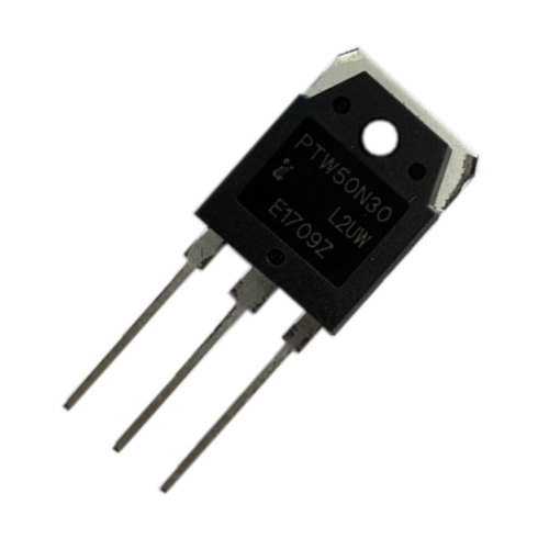


モデル: PTW50N30
供給タイプ: 元のメーカー, ODM, エージェンシー, 小売業者, その他
参考資料: 写真, データシート
VDSS: 300V
ID: 50A
Rds(on)、typ: 68mΩ
CISS: 3537pf
動作温度: -55〜150℃
Device Package: TO-3P


絶対最大 評価
|
Symbol |
Parameter |
PTW50N30 |
Unit |
|
VDSS |
Drain-to-Source Voltage[ 1] |
300 |
V |
|
VGSS |
Gate-to-Source Voltage |
±20 |
|
|
ID |
Continuous Drain Current |
50 |
A |
|
ID @ Tc =100℃ |
Continuous Drain Current @ Tc= 100℃ |
31 |
|
|
IDM |
Pulsed Drain Current at VGS= 10V[2] |
200 |
|
|
EAS |
Single Pulse Avalanche Energy |
3044 |
mJ |
|
dv/dt |
Peak Diode Recovery dv/dt[3] |
5.0 |
V/ns |
|
PD |
Power Dissipation |
305 |
W |
|
Derating Factor above 25℃ |
2.50 |
W/℃ |
|
|
TL TPAK |
Maximum Temperature for Soldering Leads at 0.063in ( 1.6mm) from Case for 10 seconds, Package Body for 10 seconds |
300 260 |
℃ |
|
TJ& TSTG |
Operating and Storage Temperature Range |
-55 to 150 |
* MOSFETは、金属酸化物 - 依存症のフィールド効果トランジスタであり、電子コンポーネントのより広いカテゴリ内の電圧制御半導体デバイスとして分類され、ゲート端子に電圧を適用することにより、ソース端子と排水端子間の電流の流れを調節します。 MOSFETは、電力管理、パワー増幅、スイッチングなど、 最新の電子機器で広く使用されています。


